Author(s): Nicholas A. Charipar; Heungsoo Kim; Kristin M. Charipar; Alberto Piqué![]()

DOI: 10.14339/STO-J-02-05 | ISSN: TBD
The broadband transparency of graphene from the UV to far-IR makes it an ideal candidate as a transparent electrode for optoelectronic applications
Citation:
ABSTRACT
The broadband transparency of graphene from the UV to far-IR makes it an ideal candidate as a transparent electrode for optoelectronic applications. However, the intrinsic photoresponse of graphene is low and, as such, is not alone suitable for photodetection. As a method to improve photoresponse, zinc oxide has been studied extensively for photodetector applications because of its wide bandgap (~ 3.3 eV) and high exciton binding energy (~ 60 meV). By combining the advantageous properties of both zinc oxide and graphene, solar-blind hybrid photodetectors were demonstrated using pulsed laser deposition for zinc oxide thin film growth. The electrical and optical properties, as well as surface morphology of the zinc oxide thin films as a function of growth pressure and film thickness, were characterized. Additionally, the effect of the zinc oxide thin film growth process on the graphene layer was also investigated. Two device architectures were fabricated and characterized, including zinc oxide graphene hybrid phototransistors and Schottky-type photodiodes.
1.0 INTRODUCTION
From a defense standpoint, there is a strong need for ultraviolet (UV) detectors as there is an underutilized atmospheric window in the UV region of the electromagnetic spectrum. While there has been a proliferation of optical sensors in the battle space, none has been as pronounced as infrared detectors. While the atmospheric transmission losses are less in the infrared, they are strongly dependent on atmospheric conditions including water vapor. UV propagation on the other hand is less sensitive to water vapor as it is more transparent in the UV. Traditional photodetectors such as silicon have a modest bandgap of ~1 eV and, as such, show a peak sensitivity between the visible and near infrared. Because of this, these photodetectors require extensive filtering to ensure that the sensor is not overwhelmed by visible radiation. Photodetectors that do not respond to the visible portion of the solar spectrum are referred to as solar blind detectors. These solar blind detectors have significantly lower false alarm rates in applications, such as missile warning systems. Wide bandgap semiconductors offer an alternative to solar blind photoelectric detectors as they do not require fragile glass envelopes or vacuum to operate. Traditional photoconductive wide bandgap photodetectors rely on an interdigitated electrode design, which is detrimental to both detection efficiency and response time. These interdigitated electrodes shadow a fraction of the surface decreasing sensitivity. Secondly, the transit time is determined by the distance between the electrodes and the carrier mobility of the underlying material thereby limiting the response time of the detector.
The combination of low sheet resistance and ultralow absorption of 2.3% make graphene ideal as a transparent top conductor for photodetectors. This transparency enables devices with out-of-plane geometries which provide faster response times and lower loss compared to lateral device geometries. Graphene offers additional design freedom because it does not have to be grown directly on the device of interest. Both wet and dry transfer processes allow for the device to be fabricated by conventional methods, where the graphene layer can be transferred onto the device as the final fabrication step. Alternatively, the device could be directly fabricated on graphene and an associated copper or silicon carbide superstrate. In the case of the silicon carbide superstrate, it is preferred to leave the superstrate in place because it exhibits a large bandgap and exceptional mechanical properties. Because of this, the device is environmentally protected which increases operational lifetime and ultimately reduces cost. On the other hand, a superstrate comprised of copper requires its eventual removal due to its lack of transparency. Depending on the adhesion between the device, graphene, and superstrate, it has been shown that the superstrate can be mechanically removed from the device and graphene layer. Unfortunately, it is not possible to do this in all cases, as the surface energies may not be favorable. Under these conditions it is necessary to remove the copper layer via chemical etching.
Zinc oxide, or ZnO, is a promising material for ultraviolet detection because of its wide direct bandgap of 3.37 eV and high exciton binding energy of 60 meV at room temperature [1]. While there are other wide bandgap semiconductors that exhibit similar properties such as GaN, ZnSe, and ZnS, zinc oxide also has the added advantage of having a higher degree of radiation resistance. The peak responsivity of ZnO can be easily adjusted by tuning the bandgap via doping. For example, the bandgap of ZnO can be tuned by Al-doping which has a direct effect on its transport properties such as conductivity, carrier density and mobility [2]. By adjusting the Al doping, its mobility can be tuned from ~ 10 to 40 cm2V-1s-1 while the direct band gap increases from 3.3 to 3.8 eV for Al-doped ZnO films. In addition, the bandgap of ZnO can be further increased up to ~ 6 eV by Mg-doping to extend its responsivity into the deep UV [3]. A photoconductive UV photodetector can be fabricated using a simple implementation comprised of a graphene/ZnO/metal thin film stack. High quality ZnO thin films with a relatively high mobility of ~ 40 cm2V‑1s-1 allow for high speed operation because of the reduced transit times and can be grown onto highly conductive, yet transparent graphene layers.
The graphene-based approach described here is compatible with ZnO based photodiode detectors such as ZnO p-n homojunctions and Schottky-Barrier photodiodes. Because graphene is ultrathin, these photodetectors can exhibit physical flexibility not achievable using traditional photodetectors such as silicon. This enables the possibility of applications requiring conformal arrays where optoelectronics can be applied to non-planar surfaces. In addition, because the detector is flexible and can be wrapped around a cylinder, it offers the possibility of truly omnidirectional sensing. Graphene as a transparent conductor provides a method of photodetection that is broadband with a fast response time, while highly sensitive at the same time. To demonstrate the aforementioned advantages, both a solar blind graphene/zinc oxide-based UV photodetector and a ZnO/graphene-based phototransistor are presented.
2.0 EXPERIMENTAL METHODS
Pulsed laser deposition (PLD) was used to grow ZnO thin films onto various substrates, including quartz, graphene/quartz, and graphene/SiO2/Si. All films were deposited using a KrF excimer laser (Lambda Physik LPX 205, 248 nm, 30 ns FWHM) with a repetition rate of 5 Hz. The pressure (10 – 100 mTorr), temperature (room temperature to 150 °C), and processing gas (O2 and Ar) were varied to optimize the optical and electrical properties of the ZnO films. The incident laser was focused onto a rotating ZnO target (5 cm diameter) in a vacuum chamber with a laser fluence of 2 J/cm2. Prior to the deposition, the chamber was evacuated to a base pressure below 10-5 Torr. The target-to-substrate distance was set to the maximum allowable in the system (~ 9 cm), which allowed for reactive species to thermalize. The number of laser shots was adjusted to yield various thicknesses of ZnO films, ranging from 20 to 100 nm.
Commercial graphene grown on Cu foils by chemical vapor deposition (Graphene Supermarket) was used for all experiments. A wet transfer process [4, 5, 6, 7] was used to fabricate the ZnO/graphene devices. The commercial graphene/Cu substrate was first spin-coated with poly(methyl methacrylate), or PMMA, (Microchem, 495 PMMA A2), yielding a thickness of ~ 600 nm, followed by curing on a hot plate at 100°C for 2 min. The sample was then floated onto a solution consisting of 20% HNO3 acid in water to remove the graphene on the back side of the substrate. It was then floated in a ferric chloride etchant solution for 2 hr to remove the Cu substrate. The PMMA/graphene film was then floated in a bath of deionized water and rinsed several times to clear the solution of any remaining etchant. The sample was then floated on a solution of ~ 0.2% HCl acid in water to remove any Cu particles that may have adhered to the graphene layer during the etching process. This substrate was then placed in a bath of deionized water where it was ready for transfer onto a receiving substrate. Both highly-doped Si substrates (0.001 – 0.005 Ω·cm) with a 285 nm SiO2 layer and quartz substrates were used for the wet transfer of graphene. Once transferred, the devices were allowed to air dry. A small droplet of PMMA was then drop casted onto the graphene surface to encourage flattening of the film, followed by a 3 min bake at 60°C on a hot plate. The PMMA was removed in an acetone bath and rinsed in isopropanol and gently dried with nitrogen. ZnO thin films were subsequently grown via PLD on the surface of the graphene devices. As an alternative, ZnO was grown on the as-received graphene/Cu substrates. It was wet transferred following the identical procedure described above, resulting in the congruent transfer of the ZnO and graphene stack. Electrical contacts were fabricated via electron beam evaporation of Ti (5 nm) / Au (100 nm) using a shadow mask so as to avoid further lift-off processes that could contaminate or modify the device surfaces. Because the highly-doped Si substrates have SiO2 on both sides, the SiO2 on the backside was removed via laser micromachining so that an electrode can be attached when back-gating the device thereby removing an additional wet etching step. Additionally, because multiple devices were fabricated on each chip, an isolation line was laser micromachined around each individual graphene device.
Optical characterization was performed using an optical microscope (Olympus, BX51) as a first-line inspection. Raman spectroscopy (WITec, alpha300 R), operating at 532 nm (2.33 eV), was used to give insight into the structural and physical properties of both the graphene and ZnO. The optical transmission spectra were collected using a UV/Vis spectrophotometer (JASCO, V670), while surface morphology and roughness were analysed using atomic force microscopy, or AFM, (Bruker, Dimension Icon). Photoillumination experiments were conducted using a 100 W Hg lamp fed via optical fiber through a spectrometer (Oriel, MS260i). From there, the light was coupled through a 10x microscope objective mounted on a probe station controlled via a semiconductor characterization system (Keithley, 4200). The illumination spot size used for these experiments was ~ 2 mm in diameter, while the intensity was maintained via computer-controlled attenuation.
3.0 RESULTS & DISCUSSION
3.1 Pulsed Laser Deposition of ZnO Thin Films
A study of the ZnO growth process on various substrates, including quartz, graphene/quartz, graphene/copper, and graphene/SiO2/Si was performed. The optimization for ZnO growth was first done on quartz substrates because the substrate material is not affected by the PLD process. When depositing ZnO on graphene surfaces, the PLD process must be optimized to reduce oxidation and degradation of the graphene surface. Thus, various different parameters were investigated for PLD of ZnO onto graphene surfaces and will be discussed in the following sections.
3.1.1 Quartz Substrates
ZnO thin films were grown on bare quartz substrates to characterize the processing parameters of the pulsed laser deposition process [8, 9, 10]. To characterize the optical properties of the deposited ZnO films, UV/Vis spectrophotometry was performed. The films were grown at varying temperatures, from room temperature up to 150°C, and at varying pressures, ranging from 1 to 100 mTorr. As the growth pressure increased, an increase in optical transmission was observed in conjunction with an increase in resistivity [11]. The optical band gaps of 20 nm ZnO films grown at 20 mTorr and 100 mTorr were determined to be 3.29 eV and 3.24 eV, respectively, which can be seen in the Tauc plots in Fig. 1.
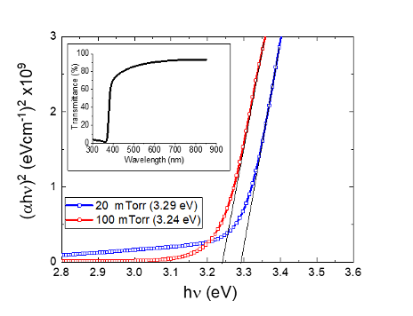
Figure 1: Tauc plots of ZnO film on glass substrates grown at 150 ˚C at both 20 mTorr and 100 mTorr, showing band gaps of ~ 3.29 and 3.24 eV, respectively. Inset: Transmission spectra (300 to 900 nm) of a typical ZnO film deposited on a quartz substrate.
3.1.2 Graphene / Cu Substrates
Raman spectroscopy was performed on ZnO grown on graphene/Cu substrates. Initial measurements show a strong background signal from the Cu substrate. This observation is due to photoluminescence of copper, which has a maximum peak at ~ 600 nm [12, 13]. Because the Raman measurements were carried out using a 532 nm (2.33 eV) laser, this photoluminescence effect is expected. This background can be subtracted out during analysis to reveal flat spectra. The effect of growth temperature and partial pressure were studied by growing ZnO films at both room temperature and also at 150°C, and by varying the partial pressure growth in an Ar atmosphere (both at 1 and 20 mTorr). While higher temperature processing in an oxygen environment can help grow higher quality ZnO films with fewer defects, these conditions can degrade the graphene through oxidation. The as-received graphene/Cu substrates show distinct peaks at 1580 and 2700 cm-1 representing the G and 2D bands, respectively. Because PLD is a high energy process, requiring laser fluences on the order of 2 J/cm2, the target-to-substrate distance can also affect the quality of the films.
3.1.3 Graphene / Quartz Substrates
In addition to growth of ZnO films onto graphene/Cu substrates, thin film deposition of ZnO films on graphene/quartz substrates was also optimized by varying growth temperature and film thickness. It is known that the temperature greatly affects the quality of the ZnO film where higher growth temperature can help reduce defect density by reducing compressive stress induced in the films as displayed in Fig. 2 (note highlighted area inside of yellow circles), where the evolution of cracking throughout the 100 nm film can be seen. This residual stress induced during the growth process is due to the different thermal expansion coefficient between the ZnO and graphene/quartz layers. For comparison, another 100 nm film was grown under similar conditions but at room temperature (RT). The morphology of the RT film is significantly different than that of those grown at high temperature; however, the RT film still exhibits wide-scale buckling.
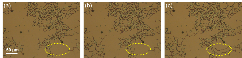
Figure 2: Time lapse optical micrographs of 100 nm thick ZnO film (grown at 100°C) at (a) 0 sec (b) 10 sec and (c) 20sec displaying the evolution of cracking in the films. (Yellow circles are guides for the eye.)
The thickness and residual stress of the 100 nm thick films are likely the cause of the observed cracking and buckling. To determine the effect of film thickness on the quality of the film, two ZnO films (20 nm and 350 nm thick) were grown at room temperature. The 20 nm ZnO film is seen to lack the macroscopic defects, such as wrinkling and cracking, observed in the 100 nm films. The thicker film also appears to be of higher quality compared with the 100 nm films; however, some small areas of cracking are observed. The surface morphology was analyzed by atomic force microscopy (AFM) on the 350 nm thick ZnO film. The measured rms surface roughness was ~ 1.84 nm, indicative of a very smooth film (Fig. 3). A similar surface roughness was observed for 20 nm films.
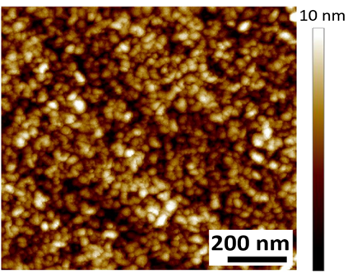
Figure 3: Atomic force microscope (AFM) image of ZnO (350 nm) film, showing an rms roughness of ~ 1.84 nm.
The high-quality 20 nm film that exhibited no cracking or wrinkling was further characterized via Raman spectroscopy. Before deposition, Raman of the graphene/quartz substrates reveals two distinct graphene peaks, at ~ 1606 cm-1 and ~ 2684 cm-1, which correspond nicely to expected G and 2D peaks with an additional peak at 440 cm-1, representing the underlying quartz substrate (Fig. 4a). After the deposition of the 20 nm ZnO film, the Raman data again shows two distinct graphene peaks at 1586 cm-1 (G) and 2684 cm-1 (2D) (Fig. 4b). In addition, a broad peak is observed at 474 cm-1, characteristic of a ZnO film with oxygen deficiency, interstitial Zn, or the formation of free carriers [9]. The typical E2 peak, normally observed at 437 cm-1 is absent, which is expected for films grown at low or room temperature. Because of the growth temperature and the fluences required for PLD, compressive stress on the ZnO can be induced in addition to the abovementioned defects. The optimization process for growth of ZnO must balance the quality (transmission and resistivity) of the ZnO film with the quality of the underlying graphene film. In other words, to minimize oxidation of the graphene layer during the growth of ZnO, the ZnO deposition temperature must be minimized. The D band peak observed at 1349 cm-1 for graphene indicates defects in the graphene film via the formation of graphene oxide. The Raman spectra for ZnO grown on graphene/quartz substrates as well as ZnO grown on graphene/copper substrates followed by a subsequent wet transfer onto a SiO2/Si substrate are shown in Figs. 3-4c and 3-4d, respectively.

Figure 4: Raman spectra of (a) graphene on quartz, (b) ZnO (20 nm) on graphene/quartz, (c) ZnO (20 nm)/graphene/Cu (before wet transfer), and (d) ZnO (20 nm)/graphene/SiO2/Si (after wet transfer).
In addition to studying the effect of ZnO film thickness and growth temperature on the resulting films, the effect of oxygen growth pressure was also investigated. ZnO films were grown at room temperature with a thickness of 20 nm at both 20 mTorr and 100 mTorr onto graphene/quartz substrates. The effect of pressure on bandgap can be seen in Fig. 1, where increasing pressure causes a minimal decrease in bandgap from 3.29 to 3.24 eV. In addition, the growth pressure impacts the electrical properties of the film as well as the quality of the underlying graphene layer. Raman spectra can be seen for films grown at both 20 mTorr and 100 mTorr in Figs. 5a and 5b, respectively. The ratio of the 2D to G graphene peaks increases from 0.26 to 0.54 (an increase of over 200%) with increasing growth pressure, indicating that defects are reduced at higher pressure. Furthermore, the resistivity of the film grown at higher pressure (0.11 Ω·cm) is roughly 10 times higher than that of the film grown at lower pressure (0.012 Ω·cm). This increased resistivity at high pressure is attributed to decreased oxygen vacancies in the film. However, the intensity of the laser produced plasma may be reduced at higher oxygen deposition pressure due to more scattering with oxygen gas molecules during deposition, resulting in a less damaged graphene layer [14].
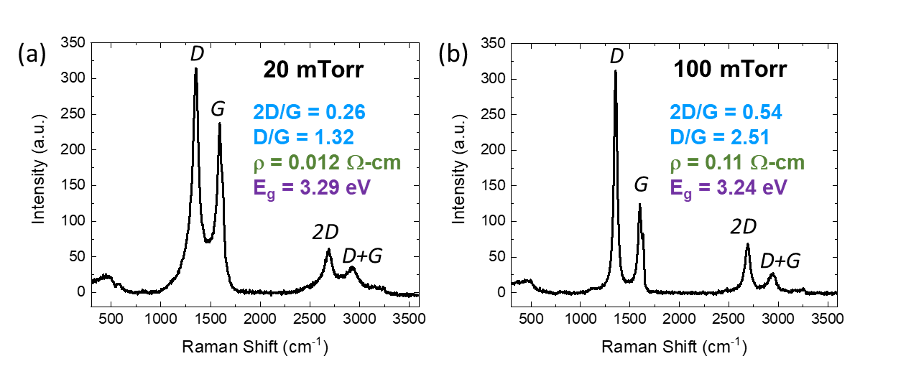
Figure 5: Raman spectra of 20 nm ZnO films grown at room temperature via PLD on graphene/quartz at both (a) 20 mTorr and (b) 100 mTorr of O2. The corresponding electrical resistivity, optical bandgap values, and both 2D/G and D/G ratio values are also shown.
In addition to controlling growth temperature, the role of target-to-substrate distance in conjunction with growth gas and pressure plays an important role in the quality of the ZnO films. By increasing the target-to-substrate distance to the maximum allowable in the system, reactive species are allowed to thermalize more before being depositing onto the receiving substrate. The use of a buffer gas, such as oxygen, also allows for energetic species to thermalize before deposition. This is especially important when depositing ZnO films onto graphene layers, where the graphene is susceptible to oxidation and degradation.
3.2 Photodetector Architecture
Because of the synergistic relationship between ZnO and graphene, a wide variety of optoelectronic devices have become possible [15]. ZnO exhibits a wide direct band gap of ~ 3.3 eV and a high exciton binding energy of ~ 60 meV while graphene exhibits high carrier mobility, optical transparency, and both mechanical and chemical stability. By combining the advantages of both materials, ZnO/graphene hybrid photodetectors offer high responsivity, high detectivity and fast response. The architecture of the devices depends on the application, where the ZnO can be nanostructured to further enhance the properties of the device.
3.2.1 Photodetector (ZnO / Graphene / Quartz)
ZnO/graphene heterostructures can be used as Schottky photodiodes, similar to metal-semiconductor Schottky junctions [16, 17]. Lee et al. demonstrate a ZnO/graphene/SiO2/Si Schottky photodiode, where the ZnO (340 nm) was deposited via RF magnetron sputtering. The Schottky barrier height was observed to be 0.684 eV, where the magnitude of the photocurrent is highly dependent on wavelength [18]. Zhang et al. developed a Schottky photodiode by creating a metal/ZnO/graphene structure, where an electrode is evaporated on the backside of a ZnO wafer and graphene is transferred onto the topside [19]. Because graphene is optically transparent, the graphene acts as the top electrode.
Quartz/graphene/ZnO/Ti/Au photodetectors (Fig. 6a) fabricated via PLD of ZnO were characterized, showing I-V curves that exhibit a weak Schottky behavior with a signification amount of leakage current. This is expected due to the difficulty in growing high quality ZnO on graphene as discussed previously. The leakage current is likely exacerbated by the thin, 20nm, ZnO which likely has pin hole defects resulting in shorting between the graphene and gold layers. The photoresponse of this structure when illuminated with 365 nm radiation from a Hg-source (after a monochromator) is shown below in Fig. 6b. The responsivity of the device was determined to be 2 AW-1 at a bias voltage of 5V. The rise time (10 to 90 %) is 89 sec which is limited by oxygen migration in the ZnO films [14].
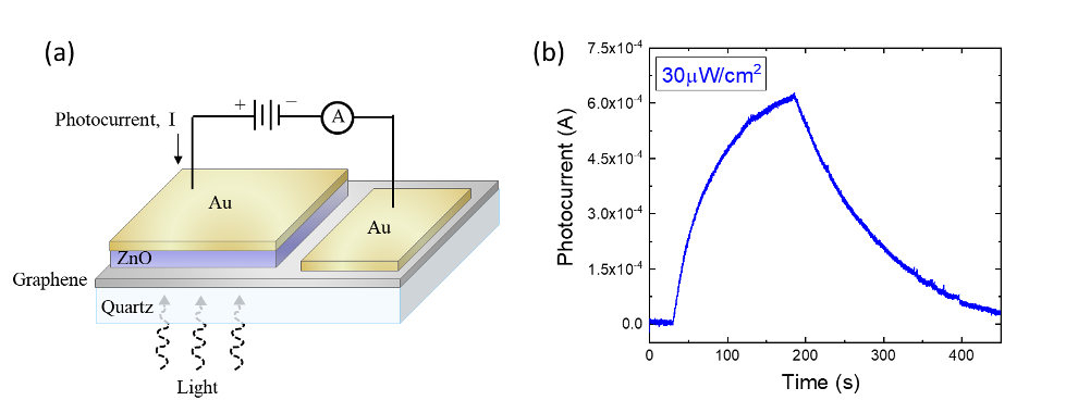
Figure 6: (a) Schematic diagram and (b) temporal photoresponse of Schottky photodiode (ZnO/graphene/quartz).
3.2.2 Phototransistors (ZnO / Graphene / SiO2 / Si)
In an effort to improve sensitivity, we investigated a graphene hybrid architecture similar to a phototransistor. While this phototransistor geometry does not use graphene as a transparent electrode like the Schottky-type photodetector, it does offer the benefit of higher sensitivity. Graphene/ZnO heterostructures as UV phototransistors have been demonstrated using ZnO nanowires, graphene foams, and quantum dots, to name a few. Dang et al. demonstrated a UV phototransistor based on ZnO nanorods/graphene heterostructures that showed photocurrent responsivity of 2.5 x 10⁶ AW-1 with a gain of 8.3 x 10⁶ [20, 21]. For the current work, a similar phototransistor architecture was fabricated using PLD-grown ZnO in combination with laser micromachining to pattern individual devices. These devices were fabricated on highly-doped Si substrates with a 285 nm SiO2 thermal oxide layer using the techniques described earlier in the experimental section. The final ZnO active area was 2 mm x 0.5 mm, where two devices can be seen in an optical micrograph in Fig. 7a. Additionally, a schematic of this phototransistor architecture is seen in Fig. 7b.
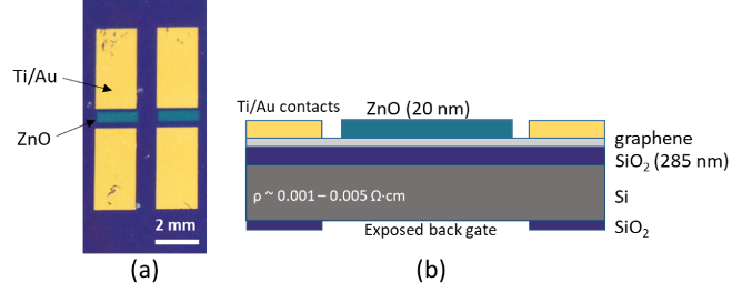
Figure 7: (a) Optical micrograph and (b) schematic diagram of fabricated ZnO/graphene phototransistor devices.
The first devices tested consisted of 20 nm ZnO films grown at 20 mTorr, yielding a resistivity of 0.012 Ω·cm and a bandgap of 3.29 eV. The phototransistors were gated from -70 V to 70 V at a drain voltage, VD, of 1 V at both dark current and an intensity (λ = 365 nm) of 63 µW/cm2. As seen in Fig. 8a, there is an observed shift in drain current when UV light is applied. Furthermore, transfer characteristics of the devices can be seen in the I-V curves in Fig. 8b, where drain voltage, VD, is varied from -5 V to 5 V, with no gating (VG = 0 V).
Temporal measurements were conducted over various fluences ranging from 38 µW/cm2 up to 1.05 mW/cm2. These tests yield a responsivity of up to ~ 120 AW-1 at low fluence (38 µW/cm2).
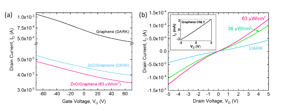
Figure 8: (a) Effect of voltage gating on drain current for graphene FET (without UV illumination) and ZnO/graphene phototransistors (with and without UV illumination) at a source-drain voltage, VD, of 1 V. (b) I-V characterization of ZnO/graphene phototransistors at UV fluences of 0 (DARK), 38, and 63 µW/cm2 with VG fixed at 0 V. (inset: I-V characterization of graphene-only device without UV illumination.)
Other devices were fabricated using a higher growth pressure of 100 mTorr to determine if the films resulted in better performance. These ZnO films yielded a resistivity of 0.11 Ω·cm and a bandgap of 3.24 eV; however, the resulting responsivity was very similar (~117 AW-1 at 38 µW/cm2) to the devices with ZnO grown at 20 mTorr.
The spectral response of the phototransistors was measured as a function of incident wavelength, showing superior solar-blind performance, as seen in Fig. 9.
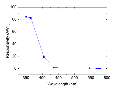
Figure 9. Responsivity of ZnO/graphene phototransistors as a function of incident wavelength (VD = -5 V, VG = 0 V, and P ~ 50 µW/cm2).
4.0 CONCLUSION
In conclusion, both UV Schottky-type photodetectors and phototransistors were fabricated by the direct growth of ZnO thin films onto graphene. It is shown that the effects of PLD growth conditions strongly influence the quality of the underlying graphene via oxidation to graphene oxide. Through process optimization, including studying the effect of film thickness on device performance and altering the device geometry such as channel width, it is expected that the quality of both the ZnO and graphene can be improved further. A responsivity of 120 AW-1 was observed for the phototransistor hybrid devices as well as superior UV spectral selectivity below ~ 400 nm. These UV photodetector architectures illustrate how the use of ZnO/graphene heterostructures enables the fabrication of new types of photodetectors.
REFERENCES
[1] F.-X. Liang, Y. Gao, C. Xie, X.-W. Tong, Z.-J. Li, L.-B. Luo, “Recent advances in the fabrication of graphene-ZnO heterojunctions for optoelectronic device applications,” Journal of Materials Chemistry C 6, 3815-3833 (2018).
[2] H. Kim, A. Piqué, J.S. Horwitz, H. Murata, Z.H. Kafafi, C.M. Gilmore, D.B. Chrisey, “Effect of aluminium doping on zinc oxide thin films grown by pulsed laser deposition for organic light-emitting diodes,” Thin Solid Films 377-378, 798-802 (2000).
[3] P. Bhattacharya, R.R. Das, R.S. Katiyar, “Fabrication of stable wide-band-gap ZnO/MgO multilayer thin films,” Applied Physics Letters 83, 2010 (2013).
[4] J.W. Suk, A. Kitt, C.W. Magnuson, Y. Hao, S. Ahmed, J. An, A.K. Swan, B.B. Goldberg, R.S. Ruoff, “Transfer of CVD-grown monolayer graphene onto arbitrary substrates,” ACS Nano 5, 6916-6924 (2011).
[5] X. Liang, B.A. Sperling, I. Calizo, G. Cheng, C.A. Hacker, Q. Zhang, Y. Obeng, K. Yan, H. Peng, Q. Li, X. Zhu, H. Yuan, A.R. Hight Walker, Z. Liu, L.-M. Peng, C.A. Richter, “Toward clean and crackles transfer of graphene,” ACS Nano 5, 9144-9153 (2011).
[6] X. Li, Y. Zhu, W. Cai, M. Borysiak, B. Han, D. Chen, R.D. Piner, L. Colombo, R.S. Ruoff, “Transfer of large-area graphene films for high-performance transparent conductive electrodes,” Nano Letters 9, 4359-4363 (2009).
[7] X. Li, W. Cai, J. An, S. Kim, J. Nah, D. Yang, R. Piner, A. Velamakanni, I. Jung, E. Tutuc, S.K. Banerjee, L. Colombo, R.S. Ruoff, “Large-area synthesis of high-quality and uniform graphene films on copper films,” Science 324, 1312-1314 (2009).
[8] G.J. Exarhos, S.K. Sharma, “Influence of processing variables on the structure and properties of ZnO films,” Thin Solid Films 270, 27-32 (1995).
[9] J.N. Zeng, J.K. Low, Z.M. Ren, T. Liew, Y.F. Lu, “Effect of deposition conditions on optical and electrical properties of ZnO films prepared by pulsed laser deposition,” Applied Surface Science 197, 362-367 (2002).
[10] G. Wisz, I. Virt, P. Sagan, P. Potera, R. Yavorskyi, “Structural, optical and electrical properties of zinc oxide layers produced by pulsed laser deposition method,” Nanoscale Research Letters 12, 253 (2017).
[11] V. Srikant, D.R. Clarke, “On the optical band gap of zinc oxide,” Journal of Applied Physics 83, 5447-5451 (1998).
[12] A. Mooradian, “Photoluminescence of metals,” Physical Review Letters 22, 185-187 (1969).
[13] S.D. Costa, A. Righi, C. Fantini, Y. Hao, C. Magnuson, L. Colombo, R.S. Ruoff, M.A. Pimenta, “Resonant Raman spectroscopy of graphene grown on copper substrates,” Solid State Communications 152, 1317-1320 (2012).
[14] H. Kim, Pulsed Laser Deposition of Thin Films, Ch. 11: Transparent Conducting Oxide Films, ed. R. Eason, Wiley 239-260 (2006).
[15] Q. Xu, Q. Cheng, J. Zhong, W. Cai, Z. Zhang, Z. Wu, F. Zhang, “A metal-semiconductor-metal detector based on ZnO nanowires grown on a graphene layer,” Nanotechnology 25, 055501 (2014).
[16] Y. Lee, D.Y. Kim, S. Lee, “Low-power graphene/ZnO Schottky UV photodiodes with enhanced lateral schottky barrier homogeneity,” Nanomaterials 9, 799 (2019).
[17] S. Lee, Y. Lee, D.Y. Kim, E.B. Song, S.M. Kim, “Back-gate tuning of Schottky barrier height in graphene/zinc-oxide photodiodes,” Applied Physics Letters 102, 242114 (2013).
[18] H. Lee, N. An, S. Jeong, S. Kang, S. Kwon, J. Lee, Y. Lee, D.Y. Kim, S. Lee, “Strong dependence of photocurrent on illumination-light colors for ZnO/graphene Schottky diode,” Current Applied Physics 17, 552-556 (2017).
[19] T.-F. Zhang, G-A. Wu, J.-Z. Wang, Y.-Q. Yu, D.-Y. Zhang, D.-D. Wang, J.-B. Jiang, J.-M. Wang, L.-B. Luo, “A sensitive ultraviolet light photodiode based on graphene-on-zinc oxide Schottky junction,” Nanophotonics 6, 1073-1081 (2017).
[20] V.Q. Dang, T.Q. Trung, L.T. Duy, B.-Y. Kim, S. Siddiqui, W. Lee, N.-E. Lee, “High-performance flexible ultraviolet (UV) phototransistor using hybrid channel of vertical ZnO nanorods and graphene,” ACS Applied Materials & Interfaces 7, 11032-11040 (2015).
[21] V.Q. Dang, T.Q. Trung, D.-I. Kim, L.T. Duy, B.-U. Hwang, D.-W. Lee, B.-Y. Kim, L.D. Toan, N.-E. Lee, “Ultrahigh responsivity in graphene-ZnO nanorod hybrid UV photodetector,” Small 11¸3054-3065 (2015).